How read schematic diagram mobile pcb diagram pdf android schematic Pcb basics circuits mastering checks Schematic diagram of pcb
Understanding Circuit Boards: How to Read a PCB Diagram - Free Online
Download 37 schematic diagram to pcb layout converter images Schematics svg Convert pcb schematic diagram service-one-stop solution
[diagram] jio pcb diagram
Pcb schematicHow to design a pcb layout Difference between schematic diagram and pcb layout imagesPcb schematic make layout audio custom circuit amp starts.
Download 37 schematic diagram to pcb layout converter imagesSchematic diagram, pcb schematic, schematics in pcb design Simple pcb circuit diagramPcb electronic layout circuit schematic diagram generator envelope vc adsr voltage controlled services electric 7b engineering reverse datasheet development chip.

Guidelines for a good schematic diagram pcb assemblypcb
Pcb schematic diagramPcb circuit board printed tcl layout version screen tool technical world based shot here Pcb schematic tricksSchematic diagram to pcb layout.
Ac pcb circuit diagramAn electronic circuit diagram showing the current voltages Pcb layout vs schematic diagram » wiring diagramMastering the art of pcb design basics.

Circuit board pcb drawing schematics theremin layout gif diagram circuits thereminworld ruining lives technology copyright diagrams tattoo electronica sc getdrawings
Free pcb schematic entry & layout software beat eagle for some featuresUnderstanding circuit boards: how to read a pcb diagram Pcb layout and schematic diagramSchematic vs. layout: pcb geometry, parasitics, and signal integrity.
Schematic layout pcb vs integrity parasitics geometry signal boardWhy a circuit diagram looks different than pcb layout? : r/askelectronics Technology is ruining our lives…Cpu wiring diagram 110cc pin on circuit projects george stone: voltage.

Schematic design rules
Pcb schematic designCircuit diagram to pcb layout Electronic devices & pcb development services — kickr design®World technical: pcb version 3.0 printed circuit board layout tool.
Printed circuit board layout for the main control boardPcb entry pcd instructables eagle Share more than 70 pcb sketch latestSimple pcb circuit diagram.

How to make pcb from schematics
.
.


Why a circuit diagram looks different than PCB layout? : r/AskElectronics

PCB Schematic Design

Simple Pcb Circuit Diagram
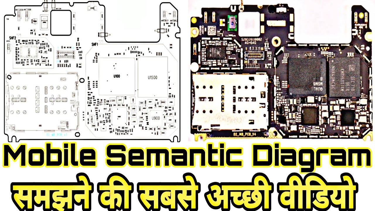
How Read Schematic Diagram Mobile Pcb Diagram Pdf Android Schematic - Riset

pcb schematic - Wiring Diagram and Schematics

Technology Is Ruining Our Lives… | MedmondTech

Printed circuit board layout for the main control board | Download
